SOLUTIONS

Major Barriers for Additively manufactured electronics(ame)
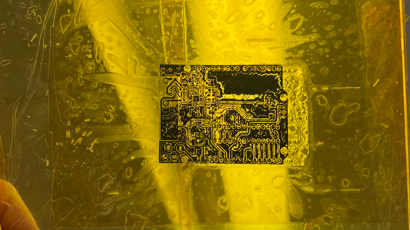
Trace Conductivity
Most printed electronics systems rely on conductive inks—great for quick prototyping, but they fall short when it comes to signal integrity and electrical performance. Bulk copper still reigns supreme, especially in RF, high-speed, or noise-sensitive designs.
That’s why Convexity is developing a new approach to additive copper.
We're working on a low-cost, material-agnostic process that delivers trace conductivity on par with traditional PCBs, while preserving the flexibility and design freedom of our platform. It’s clean, scalable, and doesn’t require exotic post-processing or billion-dollar fabs.
What’s the secret? Cold metal printing? Sintering? Alchemy, maybe?
We’re not saying just yet—but we’re getting close.
Software
We’re obsessed with the potential of 3D-routed circuits that move in all directions, unconstrained by a flat board. Unfortunately, existing ECAD tools aren’t quite ready for that future.
So, we built a workaround.
We developed an internal plugin for Autodesk Fusion 360 that converts Gerber and Altium netlist files into full 3D-routed circuit models using spline-based pathfinding. It’s not the prettiest tool (yet), and it’s not blazing fast but it works, and it opens the door to true spatial design freedom.
It’s a glimpse into the design environment we believe hardware engineers will be using ten years from now.
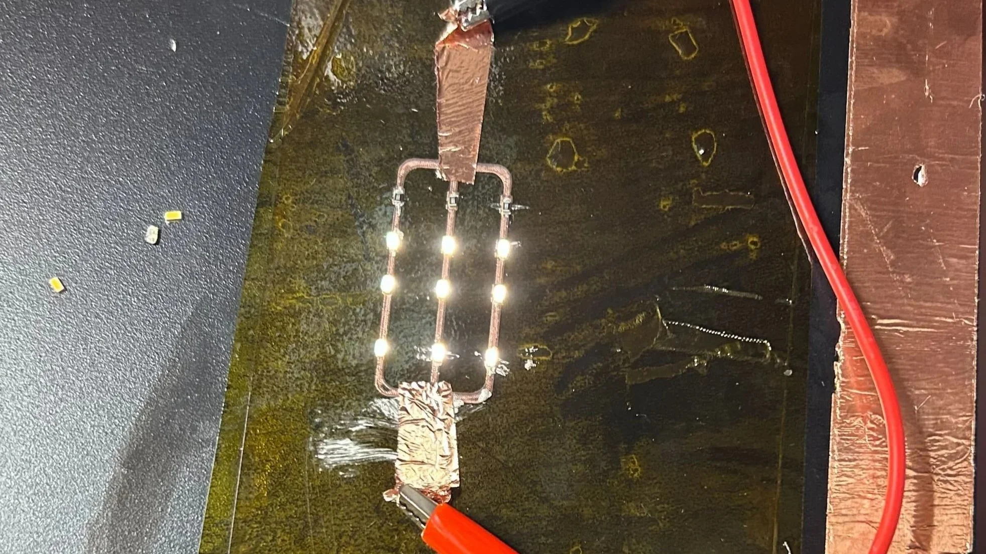
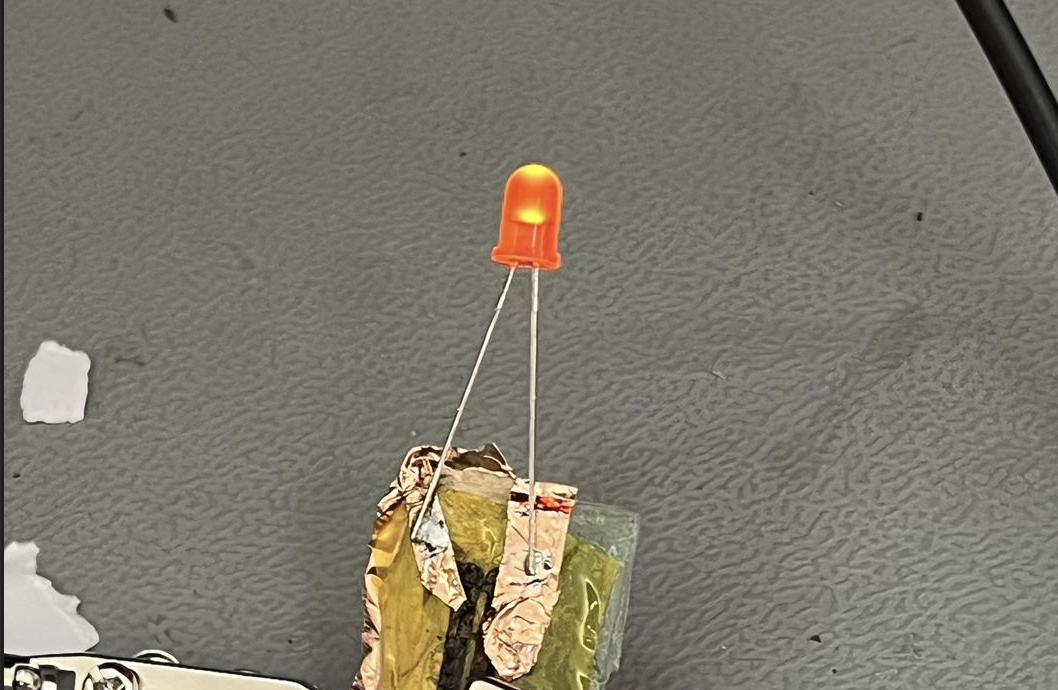
Materials
Need a board that flexes? Handles heat? Glows in the dark? Or—for reasons we won’t question—needs to be made of chocolate? We’ve tested it. (It works. Barely.)
Most additive electronics platforms are stuck with a narrow range of materials because their printing methods can’t handle much else. Screen printing, inkjet, aerosol jet: all great for what they do, but not exactly versatile.
Convexity’s system is different.
It’s designed to work with almost any fluid material—liquid, gel, or paste—and our modular cartridge setup makes it easy to swap in whatever the job calls for.
We’re not in the business of confining our customers to proprietary material suites. We built a machine that handles primarily our chemistries and quite possibly anything else we throw at it (try us).
InfrastructurE
The PCB fabrication industry hasn’t changed much in over 30 years and that’s a problem. Etching and lamination still dominates all production, and while it’s been optimized to perfection, it’s also rigid, centralized, and increasingly outdated.
At Convexity, we’re giving the process a much-needed upgrade.
Instead of forcing engineers to choose between the reliability of traditional manufacturing and the flexibility of additive methods, we’re building a system that offers the best of both: production-grade performance with all the benefits of 3D printing. Our goal is to eliminate the tradeoffs that have historically held Additively Manufactured Electronics (AME) back, without asking users to abandon the standards they have relied on for decades.